Manufacturer:KLA Corporation
Model:KLA 5105
Type:Advanced Inspection Module
Application:Semiconductor Wafer Inspection
Detection Capability:Sub-50nm Defects
Resolution:High Resolution Imaging
Software:Integrated Inspection Software Suite
Inspection Rate:Up to 200 wafers per hour
Dimensions:Width: 60cm, Height: 120cm, Depth: 80cm
Weight:Approximately 500kg
Power Requirements:220V AC, 50/60Hz
Operating Environment:Temperature: 18°C to 25°C, Humidity: 20% to 80%
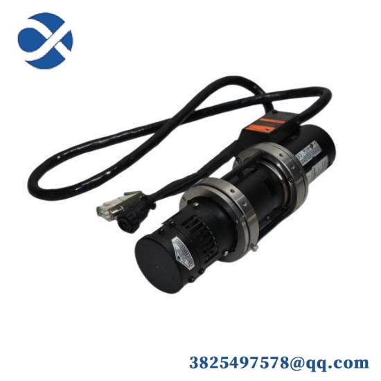
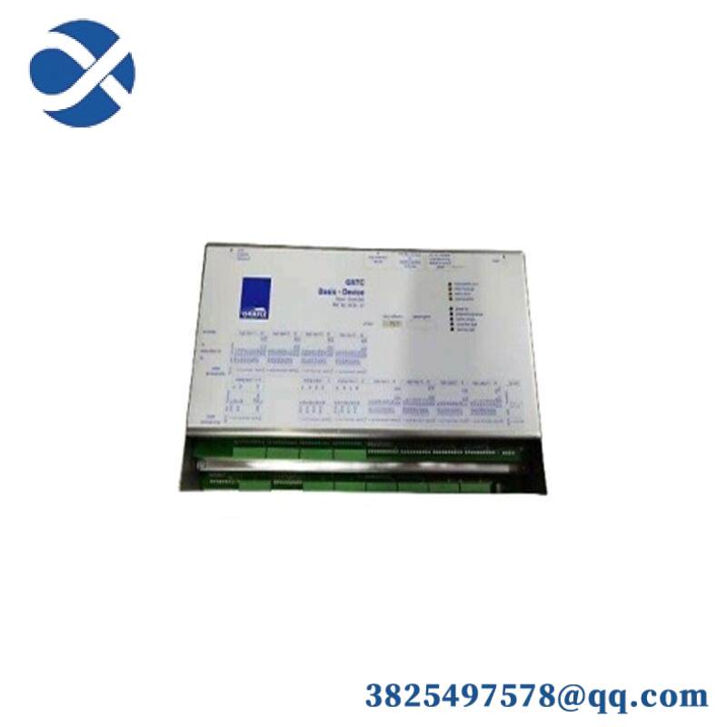
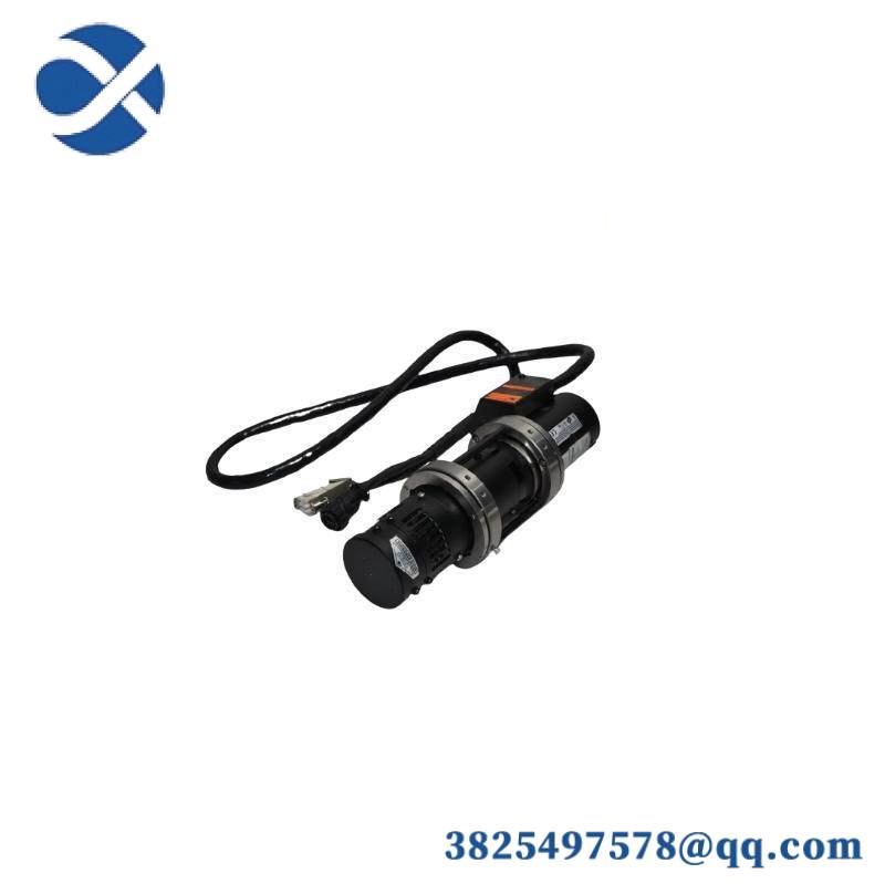
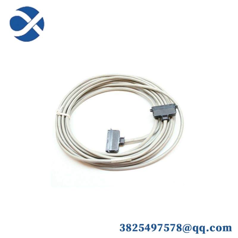
The KLA KLA 5105 Advanced Inspection Module is a cutting-edge solution for semiconductor wafer inspection. Designed for precision and reliability, this module offers sub-50nm defect detection capabilities essential for modern semiconductor manufacturing. With high-resolution imaging, it ensures that even the smallest defects are identified and corrected, enhancing overall wafer quality. The integrated inspection software suite provides a comprehensive analysis platform, allowing technicians to monitor and optimize the inspection process efficiently. Operating at up to 200 wafers per hour, the KLA 5105 is built to handle high-volume production environments. Its robust design, weighing approximately 500kg, is built to withstand the rigorous demands of continuous operation. The KLA 5105 operates within a specific environmental range, requiring 220V AC power and ensuring stable performance under controlled conditions. Ideal for semiconductor fabrication facilities, this module is a vital tool for maintaining high standards of quality and efficiency.


There are no reviews yet.